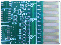

Min Line Width /
Clearance : 4/4mil
Finishing : ENIG with Hard Gold
Capability:
- Maximum Layer Count : 30 Layers
- Maximum Stack Via : 4+N+4
- Minimum Line Width : 2 mil for HDI PCB , 3 mil for conventional PCB
- Minimum Clearance : 2 mil for HDI PCB, 3 mil for Conventional PCB
- Minimum Hole Size : 0.2mm for Mechanical drill, 0.1mm for HDI
- Impedance Control PCB
- Countersunk PCB, Semi Hole.
- Copper Thickness: 1/3 oz to 6 oz
- Surface Treatment : HASL, HASL Lead Free, OSP, ENIG, Selective ENIG, ENEPIG, Immersion Tin, Immersion Silver.
- Micro via filled with Copper.

